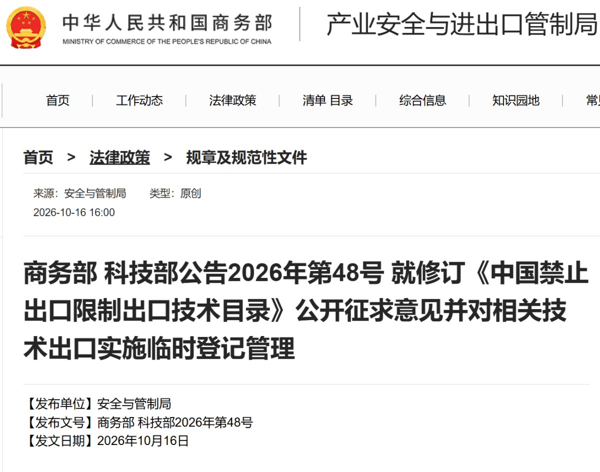
On October 16, the Ministry of Commerce publicly solicited comments on revisions to the Catalogue of Technologies Prohibited or Restricted from Export by China and implemented temporary registration management for the export of relevant technologies.This public consultation covers 40 technologies in three fields: artificial intelligence, biopharmaceuticals, and photovoltaics. The photovoltaic field includes 12 technologies related to polysilicon manufacturing, silicon wafer manufacturing, and cell manufacturing. The scope of technology management also includes key and core equipment incorporating these technologies.Among them, polysilicon preparation technology, silicon wafer preparation technology, and solar cell preparation technology are divided into two categories: prohibited exports and restricted exports.The Ministry of Commerce stated that the addition of the photovoltaic field is primarily intended to safeguard national security and interests. In recent years, photovoltaic technology has been increasingly applied in sensitive fields such as aerospace, defense, unmanned equipment, and high-security-level infrastructure. The national security risks that may arise from photovoltaic technology exports have continued to increase, making it necessary to implement timely and proportionate regulation.Serial No. | Industry Sector | Code | Technology Name | Control Parameters |
|---|
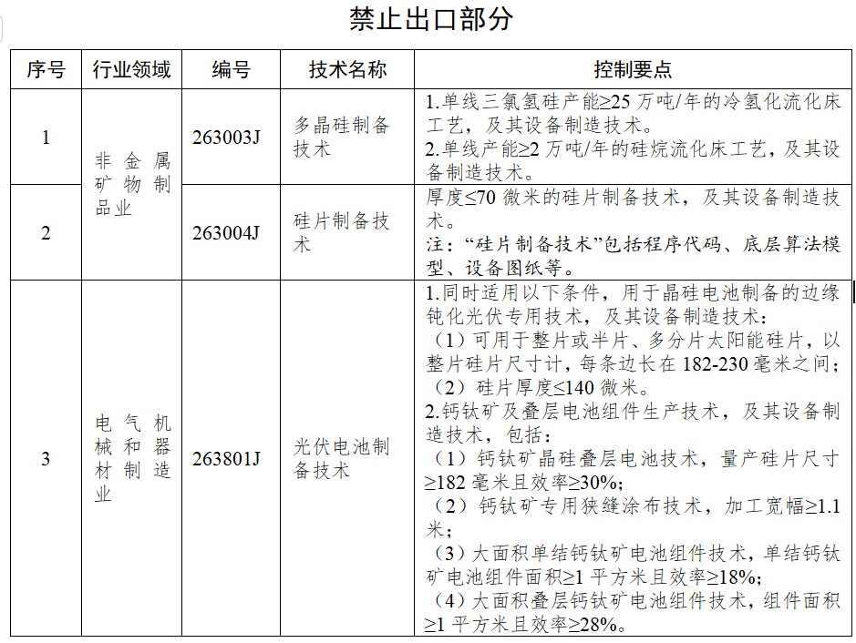
1 | Manufacture of Non-metallic Mineral Products | 263003J | Polysilicon Preparation Technology | 1. Fluidized-bed cold hydrogenation process for trichlorosilane with a single-line capacity of ≥250,000 tonnes/year, and its equipment manufacturing technology.
2. Silane fluidized-bed process with a single-line capacity of ≥20,000 tonnes/year, and its equipment manufacturing technology. |
2 |
| 263004J | Silicon Wafer Preparation Technology | Technology for preparing silicon wafers with a thickness of ≤70 μm, and its equipment manufacturing technology.
Note: “Silicon wafer preparation technology” includes program code, underlying algorithm models, equipment drawings, and the like. |
3 | Manufacture of Electrical Machinery and Equipment | 263801J | Photovoltaic Cell Preparation Technology | 1. Photovoltaic-specific edge passivation technology for preparing crystalline silicon cells that meets all of the following conditions, and its equipment manufacturing technology:
(1)Suitable for full, half, or multi-cut solar silicon wafers, with each side measuring 182–230 mm based on the dimensions of a full wafer;
(2)Silicon wafer thickness ≤140 μm.
2. Production technology for perovskite and tandem cell modules, and its equipment manufacturing technology, including:
(1)Perovskite/crystalline silicon tandem cell technology, with a mass-production wafer size of ≥182 mm and an efficiency of ≥30%;
(2)Perovskite-specific slot-die coating technology, with a coating width of ≥1.1 m;
(3)Large-area single-junction perovskite cell module technology, with a module area of ≥1 m² and an efficiency of ≥18%;
(4)Large-area perovskite tandem cell module technology, with a module area of ≥1 m² and an efficiency of ≥28%. |
Serial No. | Industry Sector | Code | Technology Name | Control Parameters |
|---|
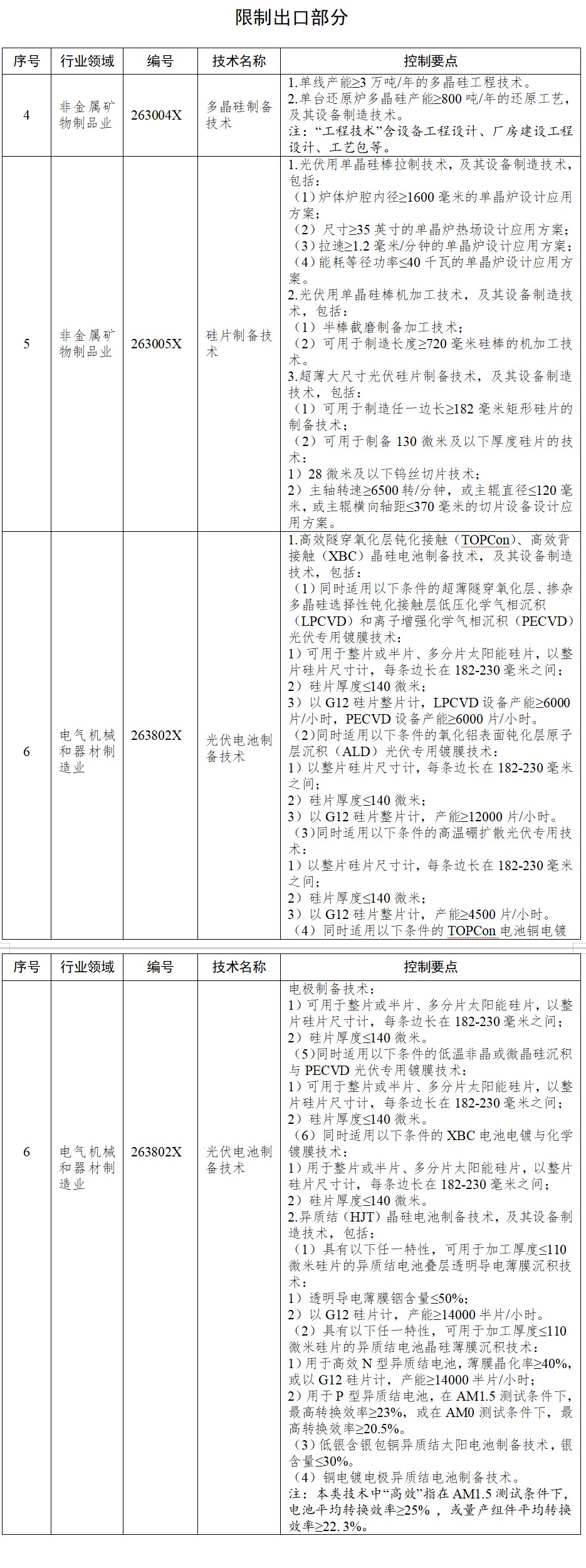
4 | Manufacture of Non-metallic Mineral Products | 263004X | Polysilicon Preparation Technology | 1. Polysilicon engineering technology for a single-line capacity of ≥30,000 tonnes/year.
2. Reduction process with a polysilicon capacity of ≥800 tonnes/year per reduction furnace, and its equipment manufacturing technology.
Note: “Engineering technology” includes equipment engineering design, plant construction engineering design, process packages, and the like. |
5 | Manufacture of Non-metallic Mineral Products | 263005X | Silicon Wafer Preparation Technology | 1. Technology for pulling monocrystalline silicon ingots for photovoltaic applications, and its equipment manufacturing technology, including:
(1)Monocrystalline furnace design and application solutions with a furnace chamber inner diameter of ≥1,600 mm;
(2)Monocrystalline furnace thermal-field design and application solutions for ingot sizes of ≥35 inches;
(3)Monocrystalline furnace design and application solutions with a pulling rate of ≥1.2 mm/minute;
(4)Monocrystalline furnace design and application solutions with an energy consumption per unit diameter power of ≤40 kW.
2. Machining technology for monocrystalline silicon ingots for photovoltaic applications, and its equipment manufacturing technology, including:
(1)Machining technology for cutting and grinding half-ingots;
(2)Machining technology suitable for manufacturing silicon ingots with a length of ≥720 mm.
3. Technology for preparing ultra-thin, large-format photovoltaic silicon wafers, and its equipment manufacturing technology, including:
(1)Preparation technology suitable for manufacturing rectangular silicon wafers with any side measuring ≥182 mm;
(2)Technology suitable for preparing silicon wafers with a thickness of 130 μm or less:
1)Tungsten wire slicing technology for wafers 28 μm thick or less;
2)Slicing equipment design and application solutions with a spindle speed of ≥6,500 rpm, or a main roller diameter of ≤120 mm, or a main roller lateral shaft spacing of ≤370 mm. |
6 | Manufacture of Electrical Machinery and Equipment | 263802X | Photovoltaic Cell Preparation Technology | 1. Preparation technology for high-efficiency tunnel oxide passivated contact (TOPCon) and high-efficiency back-contact (XBC) crystalline silicon cells, and its equipment manufacturing technology, including:
(1)Photovoltaic-specific coating technology using low-pressure chemical vapor deposition (LPCVD) and plasma-enhanced chemical vapor deposition (PECVD) for ultrathin tunnel oxide layers and doped polysilicon selective passivated contact layers, meeting all of the following conditions:
1)Suitable for full, half, or multi-cut solar silicon wafers, with each side measuring 182–230 mm based on the dimensions of a full wafer;
2)Silicon wafer thickness ≤140 μm;
3)Based on full G12 wafers, LPCVD equipment capacity ≥6,000 wafers/hour and PECVD equipment capacity ≥6,000 wafers/hour.
(2)Photovoltaic-specific coating technology using atomic layer deposition (ALD) for aluminum oxide surface passivation layers, meeting all of the following conditions:
1)Each side measures 182–230 mm based on the dimensions of a full wafer;
2)Silicon wafer thickness ≤140 μm;
3)Based on full G12 wafers, capacity ≥12,000 wafers/hour.
(3)Photovoltaic-specific high-temperature boron diffusion technology meeting all of the following conditions:
1)Each side measures 182–230 mm based on the dimensions of a full wafer;
2)Silicon wafer thickness ≤140 μm;
3)Based on full G12 wafers, capacity ≥4,500 wafers/hour.
(4)TOPCon cell copper-plated electrode preparation technology meeting all of the following conditions:
1)Suitable for full, half, or multi-cut solar silicon wafers, with each side measuring 182–230 mm based on the dimensions of a full wafer;
2)Silicon wafer thickness ≤140 μm.
(5)Photovoltaic-specific coating technology for low-temperature amorphous or microcrystalline silicon deposition using PECVD, meeting all of the following conditions:
1)Suitable for full, half, or multi-cut solar silicon wafers, with each side measuring 182–230 mm based on the dimensions of a full wafer;
2)Silicon wafer thickness ≤140 μm.
(6)XBC cell electroplating and electroless coating technology meeting all of the following conditions:
1)For full, half, or multi-cut solar silicon wafers, with each side measuring 182–230 mm based on the dimensions of a full wafer;
2)Silicon wafer thickness ≤140 μm.
2. Heterojunction (HJT) crystalline silicon cell preparation technology, and its equipment manufacturing technology, including:
(1)Transparent conductive film deposition technology for heterojunction cell stacks, with any of the following characteristics, suitable for processing silicon wafers with a thickness of ≤110 μm:
1)Indium content in the transparent conductive film ≤50%;
2)Based on G12 wafers, capacity ≥14,000 half-wafers/hour.
(2)Crystalline silicon thin-film deposition technology for heterojunction cells, with any of the following characteristics, suitable for processing silicon wafers with a thickness of ≤110 μm:
1)For high-efficiency N-type heterojunction cells, film crystallinity ≥40%, or, based on G12 wafers, capacity ≥14,000 half-wafers/hour;
2)For P-type heterojunction cells, maximum conversion efficiency ≥23% under AM1.5 test conditions, or maximum conversion efficiency ≥20.5% under AM0 test conditions.
(3)Preparation technology for low-silver-content silver-coated copper heterojunction solar cells, with a silver content of ≤30%.
(4)Preparation technology for heterojunction cells with copper-plated electrodes.
Note: In this category of technologies, “high-efficiency” means an average cell conversion efficiency of ≥25% under AM1.5 test conditions, or an average mass-production module conversion efficiency of ≥22.3%. |
6 | Manufacture of Electrical Machinery and Equipment | 263802X | Photovoltaic Cell Preparation Technology | 1. Preparation technology for high-efficiency tunnel oxide passivated contact (TOPCon) and high-efficiency back-contact (XBC) crystalline silicon cells, and its equipment manufacturing technology, including:
(1)Photovoltaic-specific coating technology using low-pressure chemical vapor deposition (LPCVD) and plasma-enhanced chemical vapor deposition (PECVD) for ultrathin tunnel oxide layers and doped polysilicon selective passivated contact layers, meeting all of the following conditions:
1)Suitable for full, half, or multi-cut solar silicon wafers, with each side measuring 182–230 mm based on the dimensions of a full wafer;
2)Silicon wafer thickness ≤140 μm;
3)Based on full G12 wafers, LPCVD equipment capacity ≥6,000 wafers/hour and PECVD equipment capacity ≥6,000 wafers/hour.
(2)Photovoltaic-specific coating technology using atomic layer deposition (ALD) for aluminum oxide surface passivation layers, meeting all of the following conditions:
1)Each side measures 182–230 mm based on the dimensions of a full wafer;
2)Silicon wafer thickness ≤140 μm;
3)Based on full G12 wafers, capacity ≥12,000 wafers/hour.
(3)Photovoltaic-specific high-temperature boron diffusion technology meeting all of the following conditions:
1)Each side measures 182–230 mm based on the dimensions of a full wafer;
2)Silicon wafer thickness ≤140 μm;
3)Based on full G12 wafers, capacity ≥4,500 wafers/hour.
(4)TOPCon cell copper-plated electrode preparation technology meeting all of the following conditions:
1)Suitable for full, half, or multi-cut solar silicon wafers, with each side measuring 182–230 mm based on the dimensions of a full wafer;
2)Silicon wafer thickness ≤140 μm.
(5)Photovoltaic-specific coating technology for low-temperature amorphous or microcrystalline silicon deposition using PECVD, meeting all of the following conditions:
1)Suitable for full, half, or multi-cut solar silicon wafers, with each side measuring 182–230 mm based on the dimensions of a full wafer;
2)Silicon wafer thickness ≤140 μm.
(6)XBC cell electroplating and electroless coating technology meeting all of the following conditions:
1)For full, half, or multi-cut solar silicon wafers, with each side measuring 182–230 mm based on the dimensions of a full wafer;
2)Silicon wafer thickness ≤140 μm.
2. Heterojunction (HJT) crystalline silicon cell preparation technology, and its equipment manufacturing technology, including:
(1)Transparent conductive film deposition technology for heterojunction cell stacks, with any of the following characteristics, suitable for processing silicon wafers with a thickness of ≤110 μm:
1)Indium content in the transparent conductive film ≤50%;
2)Based on G12 wafers, capacity ≥14,000 half-wafers/hour.
(2)Crystalline silicon thin-film deposition technology for heterojunction cells, with any of the following characteristics, suitable for processing silicon wafers with a thickness of ≤110 μm:
1)For high-efficiency N-type heterojunction cells, film crystallinity ≥40%, or, based on G12 wafers, capacity ≥14,000 half-wafers/hour;
2)For P-type heterojunction cells, maximum conversion efficiency ≥23% under AM1.5 test conditions, or maximum conversion efficiency ≥20.5% under AM0 test conditions.
(3)Preparation technology for low-silver-content silver-coated copper heterojunction solar cells, with a silver content of ≤30%.
(4)Preparation technology for heterojunction cells with copper-plated electrodes.
Note: In this category of technologies, “high-efficiency” means an average cell conversion efficiency of ≥25% under AM1.5 test conditions, or an average mass-production module conversion efficiency of ≥22.3%. |